Introductory Electronics
Semiconductors
Semiconductors are materials whose electrical conductivity lies between that of conductors and insolators. Examples include Silicon (sand), Germanium, Arsenide, Carbon, Gallium, Selenium, and compounds like Lead Sulphide.
Properties of Semiconductors
- They act as insulators at low temperatures.
- Their resistance decreases as temperature increases.
- Their electrical conductivity can be enhanced by adding impurities, a process known as doping.
Types of Semiconductors
- Intrinsic
- Extrinsic
Intrinsic Semiconductor (Pure Semiconductor)
Structure
Intrinsic semiconductors have a crystalline structure, meaning their atoms are arranged in an orderly manner. They belong to Group IV of the periodic table and have four valence electrons.
Conductivity
At temperatures below room temperature, pure germanium is a poor electrical conductor.
At room temperature, the thermal energy of valence electrons may exceed the binding energy holding them to the nucleus. When this happens, an electron becomes free, leaving behind a vacancy called a hole. A neighboring electron can then move into this hole.
The conductivity of a semiconductor increases when:
- It is exposed to electromagnetic waves of a certain maximum wavelength.
- The temperature is increased.
Carriers of Electricity
In an intrinsic semiconductor, there are two types of charge carriers:
- Free electrons - negatively charged.
- Holes - behave like positively charged particles.
Application of an Electric Field
When an electric field is applied, charge carriers move in opposite directions:
- Electrons move towards the positive terminal.
- Holes behave like positive charges and move towards the negative terminal.
Extrinsic Semiconductors
These semiconductors are produced through doping, which enhances their electrical conductivity.
Types of Extrinsic Semiconductors
- P-type Semiconductor: This type has more holes than free electrons. It is created by adding trivalent impurities such as indium or boron. Boron has three valency electrons, to form covalent bond with germanium, it can take electron from germanium, leaving a hole in germanium. This hole acts as a positive charge that can move through the crystal, The boron is called the acceptor. Conduction is due to movement of holes. The majority carrier of current are holes.
- N-type Semiconductor: This type contains more free electrons than holes. It is doped with pentavalent elements such as phosphorus or arsenic, which increases conductivity. Germanium has four valency electrons so, four of the valency electron of Arsenic forms a covalent bond with germanium. The fifth valency electron is very loosely bound, it does not participate in covalent bond. Conductivity is due to the movement of electron. The majority carrier of current are negative electrons while the minority carrier are holes.
Semiconductor Devices
- Rectifier (p-n Junction Diode)
- Photocell
- Light Emitting Diode (LED)
Rectifier (p-n Junction Diode)
A p-n junction is created by depositing an n-type material onto a clean surface of a p-type material. It functions as a current rectifier, allowing current to flow in one direction (forward bias) while permitting little to no flow in the reverse bias. This makes it useful for converting alternating current (AC) into direct current (DC).
Forward Bias
When the positive terminal of a battery is connected to the p-region and the negative terminal to the n-region:
- The positive terminal repels holes across the junction into the n-region.
- The negative terminal repels electrons into the p-region.
- This movement of charge carriers creates a forward current, resulting in low resistance and good conduction.
Reverse Bias
When the negative terminal of the battery is connected to the p-region and the positive terminal to the n-region:
- Electrons are repelled from the p-region to the n-region.
- Holes are repelled from the n-region to the p-region.
- Since there are very few free electrons in the p-region and very few holes in the n-region, the current in the reverse direction is minimal.
The p-n junction diode exhibits low resistance in forward bias and high resistance in reverse bias, making it an effective rectifier for converting AC to DC.
Advantages of p-n Junction Diode over Thermionic Diode
- Smaller in size.
- Operates with a small potential difference in radio receivers.
- No warm-up time required to generate charge carriers.
- Cheaper to manufacture and more durable.
Half-Wave Rectifier
A half-wave rectifier uses a single diode. When an AC supply is applied:
- The positive half-cycle appears at the output.
- The negative half-cycle is suppressed.
 Credit: Circuitstoday
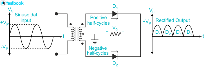
Full-Wave Rectifier
A full-wave rectifier uses two diodes (D1 and D2):
- D1 conducts during one half of the cycle.
- D2 conducts during the other half.
- The combined output forms a continuous DC voltage with fluctuations.
To smooth out these fluctuations, a filter circuit is used. This circuit consists of a high inductance in series with a large capacitor, which minimizes voltage variations.
 Credit: testbook